Circuit Floorplan
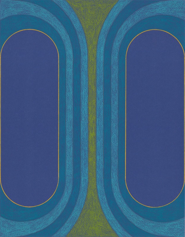
The “Circuit Floorplan” series is inspired by common symbols from electronic design. The schematic and the layout design are the two main stages in electronic board design. In the schematic stage, the circuit is drawn and verified for electrical correctness; in the layout stage, the circuit is laid out as a circuit board and verified for mechanical correctness. “Floorplaning” is a stage in between these two, where a drawing is created to indicate general areas where blocks of circuitry are to be placed on the board, thus bridging the gap between the schematic drawing and the physical layout. In this series, I have used the idea of floorplan drawings as a springboard to explore the graphic potential of electronic symbols.
-

- Circuit Floorplan #213 2019. Ink and pencils on paper. 13×10″

-

- Circuit Floorplan #202 2019. Ink and pencils on paper. 13×10″

-

- Circuit Floorplan #57 2017. Ink and pencils on paper. 13×10″

-

- Circuit Floorplan #197 2019. Ink and pencils on paper. 13×10″

-
- Circuit Floorplan #78 2017. Ink and pencils on paper. 13×10″

-

- Circuit Floorplan #27 2017. Ink and pencils on paper. 13×10″
-
- Circuit Floorplan #131 2018. Ink and pencils on paper. 13×10″

-

- Circuit Floorplan #111 2017. Ink and pencils on paper. 13×10″